Large-area CVD graphene enables photogating-based photodetection
Researchers have demonstrated that monolayer graphene offers the highest sensitivity for photogating-based photodetection due to its strong photogating modulation.
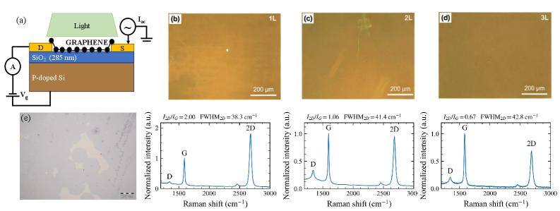
This study investigates the use of large-area chemical vapor deposition (CVD) graphene as a scalable platform for photodetectors, emphasizing the role of substrate-induced photogating in graphene/SiO2/Si structures. The research demonstrates that photoconductivity in mono-, bi-, and trilayer CVD graphene is primarily driven by photogating, with the devices responding to photon energies above the silicon band gap. The study highlights that monolayer graphene exhibits the highest sensitivity at 995 A/W, while additional layers reduce sensitivity but can enhance detectivity by lowering noise levels. The fabrication process, particularly the sequence of metal contact deposition, significantly influences the photoresponse, with devices fabricated with metal contacts before graphene transfer showing higher sensitivity.
Graphene, a fundamental two-dimensional electronic material, benefits from CVD technology, which allows for the controlled growth of uniform polycrystalline graphene layers at wafer scale. This capability opens pathways for electronic applications, as demonstrated by previous studies. The gapless nature of graphene's monolayer spectrum results in light absorption across a broad wavelength range, making graphene photodetectors promising for future optoelectronics due to their broadband operation, high carrier mobility, and compatibility with ultrafast devices.
Several mechanisms contribute to the photoresponse of graphene-based devices, including photogating, which involves light absorption in a nearby material or interface coupled to graphene. This results in a long-lived electrostatic perturbation acting as an effective gate voltage, with graphene serving as a conductive and gate-sensitive readout channel. The study underscores the importance of understanding the coexistence of multiple photoresponse mechanisms, particularly in unmodified CVD graphene on Si/SiO2 substrates.
The research demonstrates that the photoconductive response is predominantly governed by Si-induced photogating rather than direct light absorption in graphene. This conclusion is supported by the sublinear intensity dependence and the absence of response at telecom frequencies, indicating the active role of the silicon substrate in the photogating mechanism. The large sample area and gate voltage-dependent resistivity measurements confirm the dominant role of photogating, providing high sensitivity at low optical power densities.
Graphene films were grown by CVD on electrochemically polished copper foil, with the growth process carried out in a cold-wall CVD reactor developed by RusGraphene LLC. The graphene films were transferred to Si/SiO2 substrates using a wet transfer method, resulting in a large-area CVD graphene monolayer with 95% coverage. Multilayer graphene structures were obtained by repeating the transfer process, forming step-like structures with one-, two-, and three-layer regions on the same substrate.
Two fabrication routes were explored: (i) metal contacts deposited on top of graphene and (ii) graphene transferred onto pre-patterned metal contacts. The study found that the latter approach resulted in a cleaner active graphene channel and enhanced photoresponse, as it limited exposure to contact lithography and lift-off processes. The absence of a detectable photoresponse at 1550 nm further supports the substrate-induced photogating mechanism, as this wavelength does not efficiently generate carriers in the silicon substrate.
The study concludes that Si photogating is the primary photoconductivity mechanism, with the photogating mechanism allowing for a significant electrical response despite low optical absorption effects on graphene conductivity. This research highlights the potential of CVD graphene for sensitive photogating-based photodetectors, providing insights into the fabrication and operational characteristics of these devices.
Source: Graphene Feed