News14 October 2026· Graphene Feed
Mathematical graph tools uncover electronic secrets of butterfly-shaped nanographenes
GrapheneElectronicsOptoelectronicsResearch & InnovationMarket Intelligence
69 articles on Optoelectronics.
Researchers used graph theory and entropy to analyze π-electron properties in nanographene butterfly structures, revealing correlations between graph-theoretical descriptors and electronic properties with high accuracy.

Researchers have developed closed-form entropy measures for degree-based topological indices in hyper armchair carbon nanotubes.
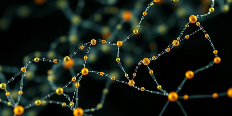
Researchers have restored light emission in bilayer 2D semiconductors using atomic stacking techniques on graphene.

Researchers at the National University of Singapore have developed a method to create laser-induced graphene circuits on kraft paper using a 355-nanometer ultraviolet laser, enabling flexible, biodegradable electronics.
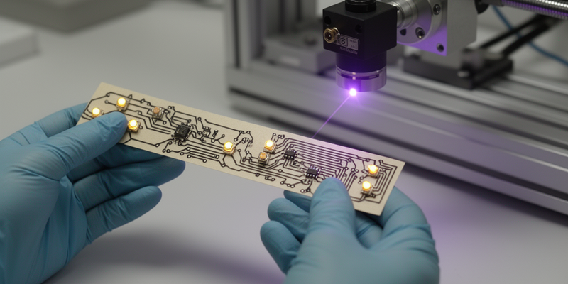
Researchers synthesized multi-walled carbon nanotube/gallium selenide nanocomposites using pulsed laser techniques, achieving a significantly altered light response.

Researchers at the University of Illinois Urbana-Champaign used coal-derived carbon nanodots to integrate high-quality dielectric layers on 2D semiconductors, achieving a leakage current density below 0.1 mA/cm².
Global Graphene Group seeks a Sales Engineer in Dayton, Ohio, to expand its graphene markets. Apply by December 31, 2026.
Researchers have developed carbon dots capable of bending light uphill, enabling optical disks to potentially store up to 400 terabits of data on a DVD-sized disk.

Researchers have published two studies cataloging nearly 9,000 two-dimensional materials, identifying over 1,600 candidates for twisting to create new quantum simulators.

Researchers have developed ultra-thin transparent electrodes using reduced graphene oxide for soft lenses, potentially transforming camera focus technology.
Researchers have developed a biomimetic nanoparticle platform using graphitic carbon nitride to control light for potential therapeutic applications.

Researchers have developed a method to synthesize nanographenes with up to eight helicenes, each with controlled handedness. This allows for precise tuning of optical and electronic properties.

The Advanced Carbons Council calls for a U.S. carbon materials innovation platform focused on standards, testing and buyer qualification. The paper links engineered-carbon supply chains to manufacturing, energy, defense and AI infrastructure. Serves as a model for governments world-wide.
Researchers discovered that using polar solvents in the modification of single-walled carbon nanotubes enhances their optical properties, enabling the detection of cholesterol.
Researchers are studying exotic quantum phases in 2D nanomaterials by twisting them into moiré superlattices, with superconductivity in graphene observed at a 1.1° twist angle.
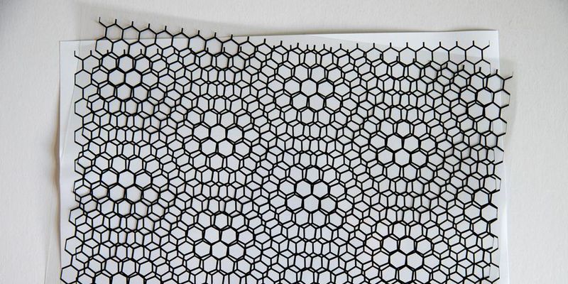
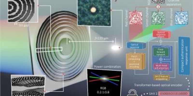
Yonsei University researchers created graphene diffractive zone plates that convert light patterns into unclonable binary security keys using a vision transformer-based model. The system shows promise for optical authentication.
Researchers led by Drexel University developed a gas-phase method to produce MXene crystals, eliminating costly and wasteful steps. This approach uses titanium tetrachloride and methane as precursors.

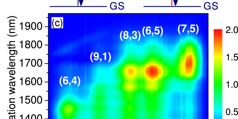
Researchers identified distinct excitonic states in single-walled carbon nanotubes using one- and two-photon luminescence excitation spectroscopy.
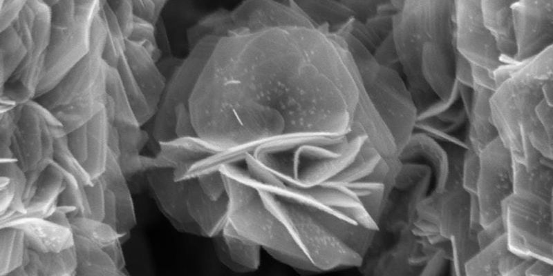
Researchers have developed a vapor-phase synthesis method to produce MXene nanomaterials, potentially reducing costs and improving scalability for electronic, environmental, and quantum technology applications.
Researchers at the National University of Singapore used 0.14-terahertz radiation to isolate electronic contributions to resistance in twisted bilayer graphene, revealing significant electron interactions at the magic angle.

The Graphene Engineering Innovation Centre offers roll-to-roll CVD systems for continuous graphene production, processing foils up to 15 cm wide at 5 metres per hour.
Researchers from Nagoya University and RIKEN developed a two-step method to synthesize diverse nanographenes, including those with rare curved structures. This method uses palladium catalysts and specific oxidants.
Researchers in the US and UK observed flexoelectricity in graphene, finding that extremely sharp bends create significant electrical polarization. This discovery aligns with theoretical predictions from 2008.

Researchers at XCT have highlighted the importance of experimental conditions in C60 cyclic voltammetry. Solvent, electrolyte, and electrode variables significantly affect the observed reduction potentials and peak shapes.
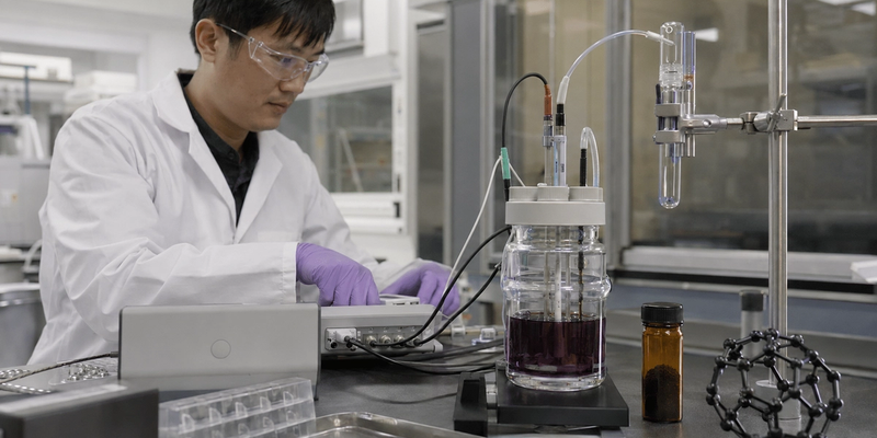
Researchers have integrated ultra-thin transparent electrodes made from reduced graphene oxide into a soft, electrically driven lens to enable focus adjustment without moving parts.
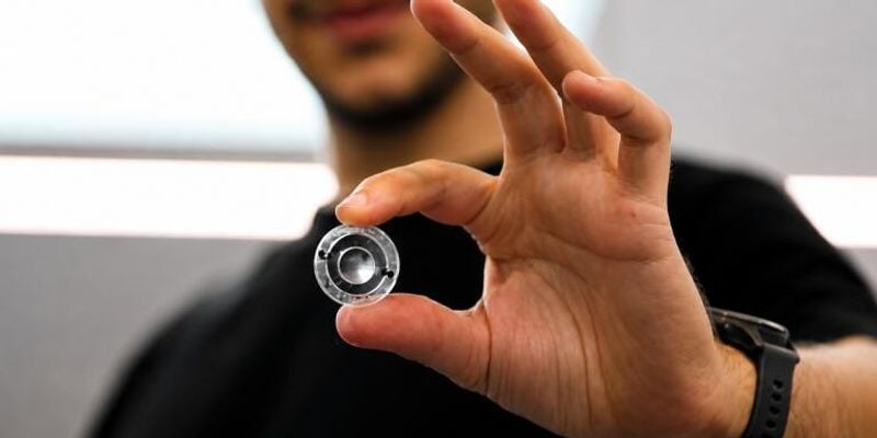
Researchers have printed an entire photodetector array by inkjet, using carbon nanotube and organic macrocycle hybrids to tell colors apart. The approach points to bendable optical sensors made without rigid silicon.
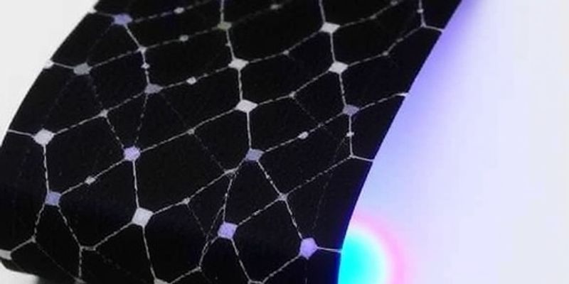
A team from Duisburg-Essen and Uppsala universities has directly observed rainbow scattering in graphene using xenon ions, confirming a previously unmeasured phenomenon.
Researchers at EPFL developed a graphene device to measure fractional electric charges in quasiparticles during the quantum Hall effect, revealing charges of one-third and two-thirds of an electron.
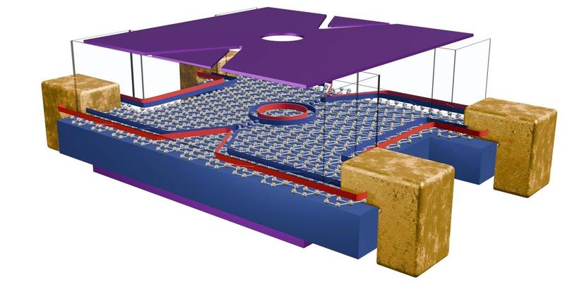
A team at the National University of Singapore has turned magic-angle twisted bilayer graphene from an insulator into a metal using only faint long-wavelength light, pointing to a new class of terahertz and far-infrared detectors.
A team from Harvard University and the University of Stuttgart theorized that valley-imbalanced rhombohedral graphene might exhibit unconventional superconductivity, potentially creating a superlattice of Cooper pairs.
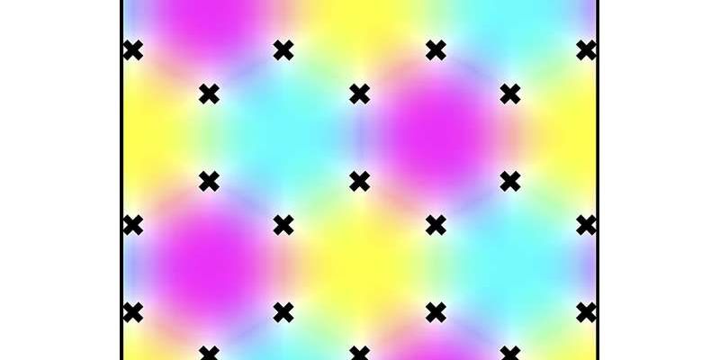
Researchers at Queen Mary University of London have developed a graphene-based soft lens that can electronically change focus without bulky parts, potentially advancing medical devices and cameras.
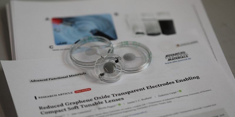
Researchers at Queen Mary University of London created compact, electrically tunable soft lenses using transparent electrodes made from reduced graphene oxide.

MIT researchers have developed a method to grow large, air-stable niobium diselenide films using graphene encapsulation. This advance could lead to more compact superconducting quantum devices.
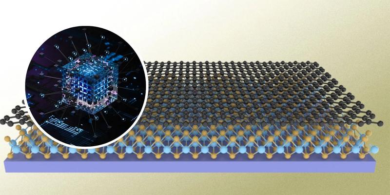
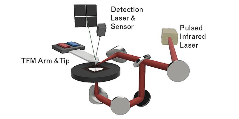
Researchers at the University of Maryland developed infrared torsional force microscopy, enabling near-nanometer precision imaging of material surfaces responding to infrared light.
Researchers at Zhejiang University developed a new synthesis method to create rare earth MXenes, yielding semiconducting and magnetic properties valuable for future electronics.
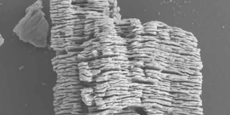
Adisyn Ltd has been granted a second U.S. patent for its graphene-coated semiconductor technology, enhancing its intellectual property portfolio.
A company led by Cambridge PhD Liu Zhenyu is advancing carbon nanotube materials for lightweight applications.

Engineers at ICFO have developed a carbon nanotube device that achieves motion control at the quantum limit through ultrastrong coupling.
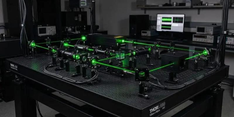
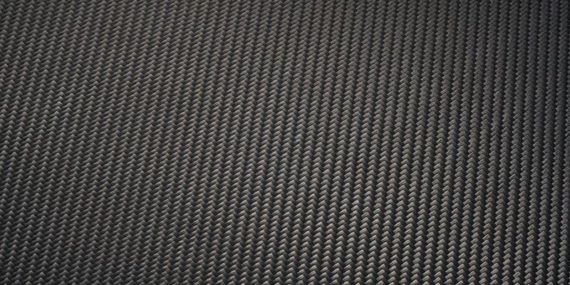
MASTERMATE is advancing carbon fiber NFC technology, enabling premium smart products with seamless digital connectivity for business, luxury, and automotive applications.
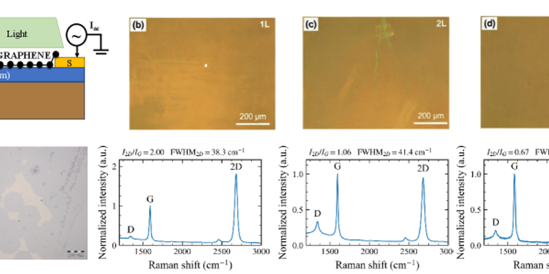
Researchers have demonstrated that monolayer graphene offers the highest sensitivity for photogating-based photodetection due to its strong photogating modulation.
Adisyn Ltd raised A$14 million through an institutional placement, signaling investor interest in its graphene-based semiconductor strategy via its subsidiary, 2D Generation Ltd.

Researchers at Fudan University developed a 2D flash memory chip using graphene that stores data with a single electron at room temperature, significantly reducing energy consumption.
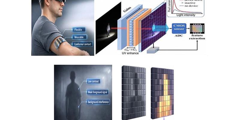
Researchers created a flexible memristor using perovskite quantum dots and graphene oxide, improving low-light image recognition by over 10% and doubling the signal-to-noise ratio.
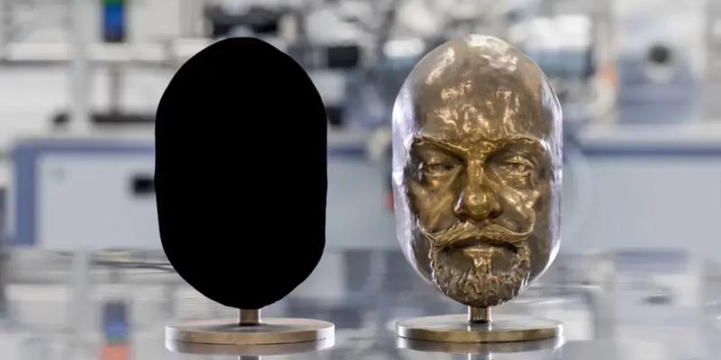
Vantablack, developed in Great Britain from carbon nanotubes, absorbs 99.965% of light, offering a potential solution to light pollution from satellite constellations like Starlink.
Researchers at Texas A&M University have developed a process to convert methane into graphene oxide using a nonthermal plasma-water interface, potentially reducing production costs.
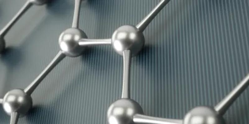
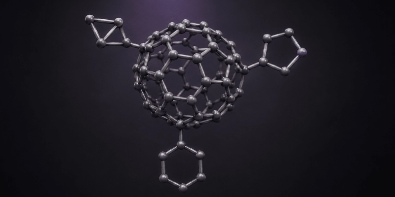
Bingel, Prato and Diels-Alder reactions each attach different groups to the C60 cage, changing solubility, electronic behaviour and how the fullerene organises with neighbouring molecules.
Researchers at the Skolkovo Institute of Science and Technology have developed a room-temperature infrared phototransistor using single-walled carbon nanotubes (SWCNTs) and lithium niobate (LiNbO3), achieving specific detectivities of up to 10^10 cm·Hz^1/2/W. This advancement in SWCNT-based pyroelectric phototransistors could lead to more affordable and portable IR sensing technologies, potentially transforming applications such as thermal imaging, environmental monitoring, and optical communications.
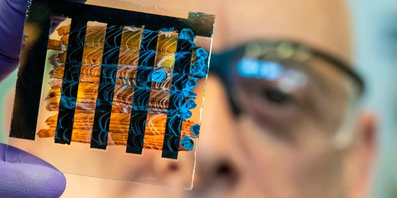
Researchers at Helmholtz-Zentrum Berlin have developed a new perovskite solar cell by incorporating graphene, enhancing its durability and efficiency. This advancement in perovskite technology could significantly reduce production costs and improve the performance of solar cells, potentially increasing the adoption of lightweight, flexible solar solutions over traditional silicon-based panels.

Researchers at the University of Modena and Reggio Emilia have demonstrated that narrow-gap carbon nanotubes function as excitonic insulators, with exciton binding energy scaling inversely with tube radius. This finding is significant for the study of carbon nanotubes, as it reveals the potential for spontaneous exciton condensation, which could influence the electronic properties and applications of these materials in advanced carbon technologies.
Researchers have optimized reduced Ti3C2 MXene to achieve a photothermal conversion efficiency of 91.66% under an 808-nanometer laser. This enhancement in free electron concentration can significantly improve MXene's performance in photothermal applications, potentially impacting fields like energy conversion and thermal management.
Researchers from the Skolkovo Institute of Science and Technology have developed a new infrared sensor using single-walled carbon nanotubes, which shows a conductivity change 10,000 to 100,000 times more pronounced than graphene. This advancement could lead to more sensitive and compact thermal cameras and medical sensors, leveraging the unique properties of carbon nanotubes for enhanced infrared detection without the need for cooling.
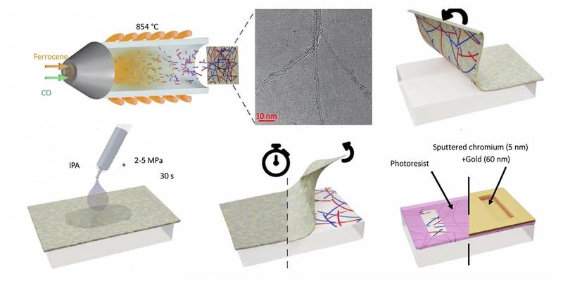
Researchers at City University of Hong Kong reached 20.5% power conversion efficiency in an organic solar cell by recovering normally non-emissive triplet excitons as extractable charge carriers.
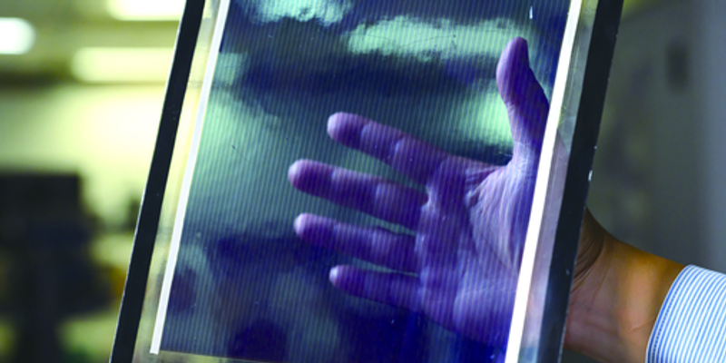
Researchers at Peking University have developed the first all-carbon nanotube CFET digital logic circuits, achieving highly balanced electrical performance between p-type and n-type transistors. This advancement is significant for the future of carbon nanotube technology, as it introduces a new path for high-density computing architectures in artificial intelligence and edge computing applications.

Physicists at Martin Luther University Halle-Wittenberg have demonstrated that carbon nanotori, specifically C₁₂₀, C₁₄₄, and C₁₆₈, can generate and control toroidal dipole moments, offering a third control channel for quantum computers with zero crosstalk. This discovery is significant for quantum computing as it introduces a new method for qubit control that is orthogonal to existing electric and magnetic control methods, potentially reducing errors caused by crosstalk in superconducting quantum processors.
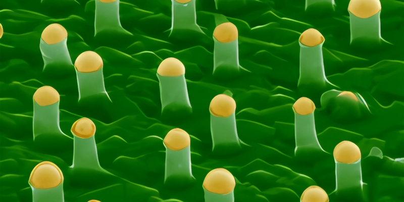
Researchers at the Vietnam Academy of Science and Technology have developed a sensor electrode using a composite material of graphene, carbon nanotubes (CNTs), and gold nanoparticles that can detect pesticide residues at concentrations as low as parts per billion (ppb). This advancement is significant for the field of advanced carbon materials as it enhances the sensitivity and functionality of sensors, contributing to improved agricultural product monitoring and food safety.
Researchers have identified several uses for Fullerene C70 in organic photovoltaics, organic electronics, and advanced nanomaterials, noting its unique elongated carbon cage structure and electron-accepting behavior. This matters because C70's distinct optical and electronic properties, compared to C60, make it a valuable material for studying and optimizing charge transport and light absorption in these advanced carbon-based applications.
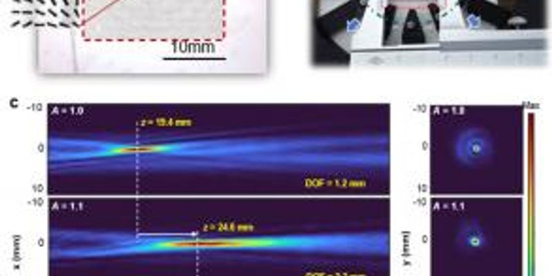
Researchers from China and Russia have developed stretchable metasurfaces using single-walled carbon nanotube (SWCNT) film, achieving dynamic terahertz wavefront manipulation at 0.35 THz. This advancement is significant for the development of smart, wearable THz components in 6G communication and intelligent sensing applications.
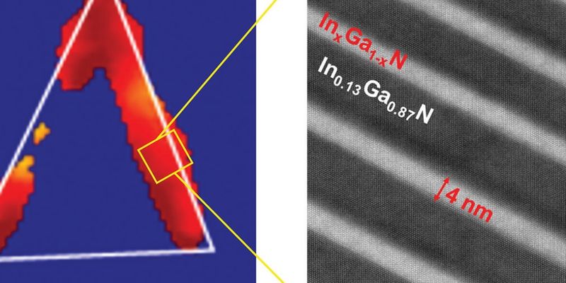
Researchers at CEA-Leti and CRHEA/CNRS grew InGaN nanopyramids through a patterned graphene monolayer on SiC, achieving red, green, and blue emission from a single epitaxial growth with an indium content up to 45 percent in the quantum wells. The approach uses graphene as a selective-area growth mask to produce relaxed InGaN pseudo-substrates, addressing the long-standing efficiency drop in InGaN-based red emitters that has blocked monolithic full-colour microLED integration for AR displays.
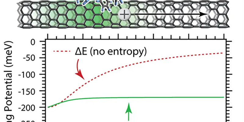
Researchers at the Netherlands Lattice Research (NLR) have demonstrated that entropy can facilitate charge separation in single-walled carbon nanotubes (SWCNTs) by attaching a negatively charged dodecaborane structure. This finding could enhance the efficiency of carbon nanotube-based semiconductors, potentially impacting electronics and energy applications.
Researchers studied the electro-optic properties of graphene oxide liquid crystals (GO-LCs) dispersed in organic solvents, extending prior work beyond aqueous systems. The findings are relevant to the graphene sector as they inform the development of GO-LC-based low-power display and electro-optic device applications.
European semiconductor companies raised substantial funding in 2025, with the ten largest rounds ranging from NXP Semiconductors' €1 billion EIB loan down to IQE's £18 million convertible note, spanning AI chips, photonics, power electronics, memory, and chip cooling. Two graphene-focused companies, Paragraf ($55M Series C) and CamGraPhIC (€25M Series A), secured funding to scale graphene-based electronic devices and graphene silicon photonics respectively, signaling continued investor commitment to graphene's commercial role in semiconductors and optical interconnects.

Researchers applied the Small Perturbation Method to analytically and numerically model how Gaussian surface roughness affects bistatic scattering coefficients, transmission coefficients, and shielding effectiveness for copper and graphene slabs across radio-frequency to near-infrared ranges. The findings provide design guidelines for tuning graphene-based shielding and optical devices by adjusting chemical potential, temperature, and layer count alongside surface roughness parameters.
Researchers integrated carbon nanotubes into an on-chip topological photonic system to enable electrical tuning of photonic properties. This demonstrates a functional role for carbon nanotubes in reconfigurable photonic devices, expanding potential applications beyond electronics and conventional optical components.
Professor Roman Gorbachev at the University of Manchester received a £1.9 million EPSRC Open Fellowship to lead a five-year project scaling van der Waals 2D material heterostructures from micrometre samples to wafer-scale fabrication using a new ultra-high vacuum platform. The work directly advances graphene and 2D materials manufacturing by targeting industrial-process compatibility and establishing a UK fabrication hub accessible to academic and industry users.

Fullerene C60, a cage-like carbon nanomaterial discovered in 1985, is under active research for applications in organic electronics, photovoltaics, lubricants, coatings, biomedical systems, and perovskite/silicon tandem solar cells. Within the advanced carbon materials sector, C60 occupies a distinct niche from fiber- or graphene-based materials, with its electron-accepting properties and molecular tunability driving continued interest in energy and specialty coating applications.
Researchers at the University of Johannesburg fabricated a three-layer nanocomposite photocatalyst (Ti1.33N@BiVO4/GdIn2Se3) incorporating a custom-synthesized MXene, achieving 20× greater electrical conductivity and charge-carrier lifetimes up to 59.5 seconds compared to single-component baselines. The MXene engineering approach demonstrates a pathway for improving charge-carrier retention in 2D carbon-adjacent materials, with direct relevance to MXene-based composite development for energy and environmental applications.

Scientists at the Hefei Institutes of Physical Science demonstrated a graphene-based terahertz modulator achieving 92% modulation depth at 0.4 THz and switching speeds approaching 100 GHz, with results published in Nature Photonics. The device's fabrication in standard semiconductor cleanroom processes positions graphene as a viable material for scalable 6G wireless components operating in the terahertz band.

The University of Exeter's Centre for Graphene Science demonstrated a graphene-zinc oxide heterostructure UV photodetector with an 8-nanosecond response time at 365 nm, 10x faster than commercial silicon devices, as published in Advanced Materials. The result advances graphene's case as a functional material in high-speed optoelectronics, with Hamamatsu Photonics engaged for industrial-scale validation and patents filed across three jurisdictions.

Researchers at the Indian Institute of Science published a graphene quantum dot LED achieving 23% external quantum efficiency in the blue spectrum in Nature Photonics, using sulfur-functionalized, size-controlled graphene quantum dots to reduce non-radiative recombination. The result advances graphene quantum dots as viable blue emitters for display applications, with the team already collaborating with Samsung Display on integration into commercial display stacks.