Printed graphene interconnects and vias for flexible hybrid electronics
Researchers at Gachon University review printed graphene interconnects and vias made from reduced graphene oxide, a route to wiring flexible hybrid electronics without conventional metal deposition.
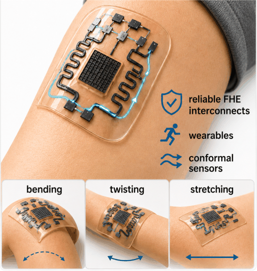
Graphene-based inks are gaining traction as a mechanically resilient alternative to silver and copper nanoparticle systems for printed interconnects in flexible hybrid electronics (FHE). Unlike brittle metallic films, graphene flake networks withstand repeated bending through crack bridging and percolation reconfiguration. However, the gap between intrinsic and practical conductivity remains a key challenge: inter-flake junction resistance results in printed film conductivity far below that of bulk metals. This review explores graphene ink formulation, including liquid-phase exfoliated, electrochemically exfoliated, and reduced graphene oxide sources, alongside inkjet, aerosol jet, screen printing, gravure printing, and electrohydrodynamic (EHD) printing strategies. Via formation, often overlooked in existing literature, is examined with a focus on sidewall coverage, aspect ratio constraints, and hybrid graphene–metal approaches. Conductivity enhancement routes, mechanical fatigue under cyclic bending, and integration with thinned silicon dies are also discussed. The review provides practical guidelines for ink selection, printing optimization, and via engineering in FHE.
The electronics industry is transitioning from traditional rigid geometries to complex, soft, and conformable architectures. This shift is driven by the need for devices that can interface seamlessly with biological surfaces, such as the human body, or wrap around irregular structures for structural health monitoring. Flexible Hybrid Electronics (FHE) combines the high-performance computation and communication capabilities of rigid silicon integrated circuits with the scalability and mechanical compliance of printed circuitry. This hybridization addresses the trade-off between the high charge-carrier mobilities of monocrystalline silicon and the low-cost, large-area manufacturability of solution-processed electronics. The resulting systems, ranging from wearable health monitors to conformal IoT sensors, require a design approach balancing electronic performance with mechanical durability.
Despite progress in FHE, interconnection networks remain a critical weak link in system-level reliability. Interconnects and vertical interconnection accesses (vias) must carry substantial current densities and survive repeated bending, twisting, and stretching without failure. This challenge involves thermo-mechanical coupling and mismatches in the coefficient of thermal expansion and elastic modulus between rigid dies and flexible substrates. Complex redistribution layers and fan-out structures are required to interface micro-scale contact pads of thinned silicon dies with macro-scale printed traces. These structures often serve as stress concentrators, inducing high shear and normal stresses that lead to delamination and circuit breakage.
Conventional solutions have relied on silver and copper nanoparticle inks, but these materials face physical limitations. Silver nanoparticle inks, while popular for their high conductivity and oxidation resistance, are brittle at the system level and exhibit channel cracking at low strains. Printed metallic tracks are also susceptible to electromigration at high current densities. Copper nanoparticle inks offer a lower-cost alternative but suffer from rapid oxidation, forming insulating oxide layers that degrade electrical performance and require high-temperature sintering processes incompatible with low-thermal-budget substrates.
Graphene, an atomically thin 2D honeycomb lattice of carbon atoms, has emerged as a potential solution to these deficiencies. Graphene's charge carriers mimic relativistic particles, enabling high carrier mobilities and near-ballistic transport. Its mechanical flexibility and exceptional strength allow it to sustain elastic strains without loss of functionality. Graphene's chemical inertness provides stability against oxidation, and its structure prevents electromigration at moderate current densities. Conductivity can be tuned through chemical doping or hybridization with metallic fillers, which bridge flake-to-flake junctions and reduce contact resistance.
However, integrating graphene into FHE faces the conductivity gap challenge. While pristine graphene is highly conductive, solution-processed printed graphene networks exhibit conductivities significantly lower than bulk copper. This discrepancy arises from high resistance at flake-to-flake junctions and insulating polymer residues from ink formulation. Addressing this "central tension"—maintaining graphene's mechanical and chemical advantages while enhancing conductivity—is the focus of current research.
The discussion is organized around the practical demands of FHE interconnects. It covers ink formulation, printing method selection, and via formation, which is the least developed area in graphene interconnect literature. Conductivity enhancement and mechanical reliability are also discussed. Graphene's role is as a passive conductor, not as a transistor channel or sensing material.
Performance criteria for FHE interconnects include power distribution and signal routing. Power distribution lines should have sheet resistance below 1 ohm/sq to avoid ohmic losses, while signal routing can tolerate up to 10 ohm/sq. Conventional copper-based interconnects set a benchmark of ~50 m.ohm/sq at 1 µm thickness, much lower than graphene interconnects. To close this gap, optimization based on sp2 network density and multipass printing is necessary.
Electromigration resistance is crucial for FHE interconnects. At high current densities, atomic migration can lead to void formation, affecting circuit operations. Graphene inks are resistant to electromigration due to strong covalent C=C bonds. Mechanical requirements vary by application, with wearable electronics needing higher strain tolerance. Fully stretchable systems demand endurance over 10,000 bending cycles at a 5 mm radius. Graphene's flexibility and high aspect ratio help bridge gaps during deformation.
Adhesion to flexible substrates like polyimide and PET is vital. Van der Waals forces and mechanical interlocking should work together, and surface tension of conductive ink should match substrate surface energy. Liquid phase exfoliation remains viable for producing large quantities of graphene inks. Electrochemical exfoliation offers high conductivity but faces scalability challenges. Reduced graphene oxide is scalable but has lower conductivity due to residual oxygen groups.
Graphene ink formulation balances ink rheology and stability. Exfoliation solvents like NMP and DMF match graphitic materials' solubility parameters but face regulatory restrictions. CyreneTM is a potential green solvent with better solubility parameters. Ink preparation involves transferring exfoliated graphene to a solvent-binder-additive system. The choice depends on the target substrate and thermal budget. Inkjet printing requires specific viscosity and surface tension parameters for stable jetting behavior.
Aerosol jet printing accepts a wider viscosity range than inkjet, but atomization mode affects usability. The fluid mechanics of inks differ by printing method, requiring optimization of ink properties.
Source: Graphene Feed