Computer-controlled electricity shapes flat nanofilms into 3D structures quickly
Researchers at Nagoya University have developed a technique to dynamically reshape graphene oxide nanofilms using computer-controlled electricity. This advancement could enhance the versatility of graphene-based materials in applications requiring precise 3D structures.
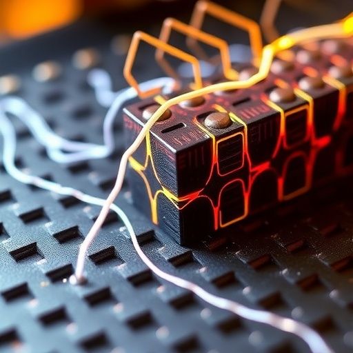
Researchers at Nagoya University have developed a method to reshape graphene oxide nanofilms in water using a computer-controlled electron beam. This technique allows for the rapid formation of dome-shaped protrusions, which can be adjusted or reshaped, offering new possibilities in nanoscale manipulation and device fabrication.
The process utilizes a 'virtual cathode,' where an electron beam scans a silicon nitride (SiN) membrane along pre-determined paths, creating an ultra-localized electric field with nanoscale precision. This approach surpasses traditional methods that depend on fixed electrodes, offering more flexibility in electrode placement and deformation scale.
The nanofilm consists of a multilayer of pyrene-linked graphene oxide, approximately 45 nanometers thick, attached to the SiN membrane. In water, the film has a negative surface charge. When exposed to the electron beam's localized negative charge, electrostatic repulsion occurs between the graphene oxide layers and the SiN substrate, causing the film to bulge into a controlled dome shape.
The separation of graphene oxide layers activates fluorescence, allowing researchers to monitor nanoscale changes in real-time through optical interference patterns. This optical feedback provides insights into dynamic height changes that were previously undetectable.
Experimentally, dome protrusions 1,200 nanometers high and 37 micrometers wide were formed within seconds, outperforming light-based methods. The deformations are reversible but occur asymmetrically; swelling under the electron beam is faster than relaxation once the beam is off. This is due to rapid dielectric polarization buildup in the SiN layer and slower dissipation of surface charge.
By adjusting beam intensity and duration, and overlapping deformed regions, researchers created complex 3D surface features. Repeated reconfiguration at the same site was possible without degrading the film, demonstrating robust reprogrammable nanoscale actuation.
As a practical demonstration, the bulged nanofilm moved a 10-micrometer polystyrene bead through water using minute pushing and electrostatic forces. Although preliminary, this suggests potential for manipulating microscale particles, possibly leading to nanoscale robotic manipulation or cellular guidance.
The research team believes this technology could enhance integration between computers and nanomachines by enabling on-demand generation of surface irregularities crucial for controlling friction, adhesion, and assembly at microscopic scales. Challenges remain, such as precise control of film delamination and operation in physiological electrolytes, but the potential for programmable nanomachine interfaces has advanced significantly.
Source: Graphene Feed