Carbon atoms mapped in 3D with record precision in twisted bilayer graphene
Researchers mapped all 6,648 carbon atoms in twisted bilayer graphene with 0.12 ångström precision using ptychographic atomic electron tomography, revealing detailed atomic-scale structural variations.
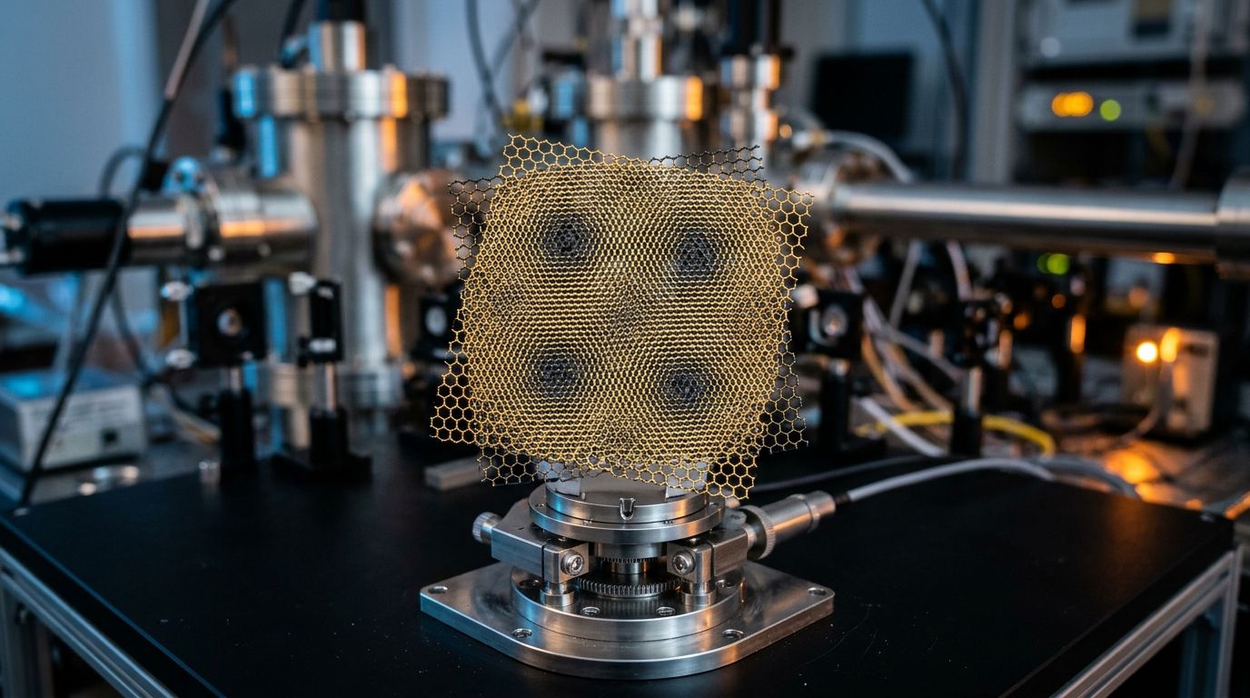
Researchers have achieved a groundbreaking feat by mapping all 6,648 carbon atoms in a twisted bilayer graphene sample in three dimensions with a precision of 0.12 ångströms. This study, published in Nature Nanotechnology, utilized a technique known as ptychographic atomic electron tomography (pAET) to provide the most detailed three-dimensional visualization of individual light atoms in a material. This advancement is significant for understanding the atomic-scale structure and properties of light-element materials.
Ptychography, the underlying method, is a computational microscopy technique that merges crystallography and microscopy by integrating coherent diffraction patterns with iterative phase retrieval. While multislice electron ptychography is known for achieving deep-sub-ångström lateral resolution in two dimensions, its depth resolution has typically been limited to the nanometre scale, insufficient for tracking the vertical positions of single atoms. Previously, pAET enabled three-dimensional atomic structure determination in nanomaterials, but resolving individual light atoms like carbon, which weakly scatter electrons, posed a significant challenge.
The research team selected twisted bilayer graphene as a model system to overcome this challenge. This material consists of two atomically thin carbon sheets stacked with a slight rotational twist, creating a moiré supercell that modulates the local atomic environment. By acquiring diffraction data and reconstructing the three-dimensional atomic structure, the researchers localized all 6,648 carbon atoms with 0.12 ångström precision. This accuracy is sufficient to detect subtle vertical displacements of atoms, which are approximately 1.4 ångströms apart in the graphene lattice.
The 3D atomic structure revealed that the interlayer spacing between the graphene sheets is not uniform. Instead, the spacing and corrugation, or the gentle undulation of the sheets, vary systematically across the moiré supercell based on the local stacking arrangement of the atoms. In specific alignments, the layers either pull closer together or bow apart, forming a landscape of atomic-scale hills and valleys dictated by stacking-dependent interlayer interactions. This visualization confirms how the geometry of twisted van der Waals materials is shaped by the interplay between twist angle and stacking order.
Beyond the corrugations, the study identified chiral lattice distortions with distinct topological characteristics. The researchers observed displacement textures resembling merons, anti-merons, and anti-skyrmions, which are spin-like patterns familiar from magnetism, appearing in the structural distortions of the carbon lattice. These chiral textures, quantified through three-dimensional displacement vectors of individual atoms, demonstrate that the lattice of twisted bilayer graphene forms handed, vortex-like patterns at the nanometre scale, a phenomenon predicted theoretically but now imaged experimentally.
The study also identified local defects within the moiré material. The three-dimensional atomic positions allowed the team to characterize three silicon dopant atoms and one carbon vacancy embedded in the graphene lattice. This capability to locate isolated impurities and missing atoms and determine their local environments in three dimensions is crucial, as dopants and vacancies significantly influence the electronic behavior of graphene-based devices.
To explore the implications of the experimentally derived structure, the researchers conducted density functional theory calculations based on the measured atomic coordinates. These calculations predict electronic band narrowing and the opening of a gap at the K point of the electronic band structure compared to a relaxed theoretical model. The subtle structural distortions captured by the imaging, such as corrugations and chiral displacements, are expected to impact the electronic properties, highlighting the importance of using experimentally determined atomic structures rather than idealized models when predicting the behavior of moiré materials.
Multislice pAET simulations suggest that this method can be extended beyond graphene. The calculations support applying the technique to diamond containing a nitrogen–vacancy center, a defect of interest for quantum sensing and quantum information technologies, and to amorphous carbon, where the disordered arrangement of atoms has long resisted precise three-dimensional characterization. Extending pAET to these systems would bring the same atom-by-atom 3D precision to materials central to quantum technologies and the study of disordered light-element networks.
This work establishes ptychographic atomic electron tomography as a practical tool for three-dimensional imaging of individual carbon atoms. It demonstrates, in a single model system, how stacking-dependent corrugations, chiral lattice distortions, dopants, and vacancies shape the atomic landscape of a moiré material. By linking the experimentally determined 3D atomic structure to predicted electronic behavior, the study marks progress toward understanding how the precise positions of individual light atoms contribute to the macroscopic properties of materials.
Source: Graphene Feed