Scientists develop ultrathin superconductors for compact quantum devices
MIT researchers have developed a method to grow large, air-stable niobium diselenide films using graphene encapsulation. This advance could lead to more compact superconducting quantum devices.
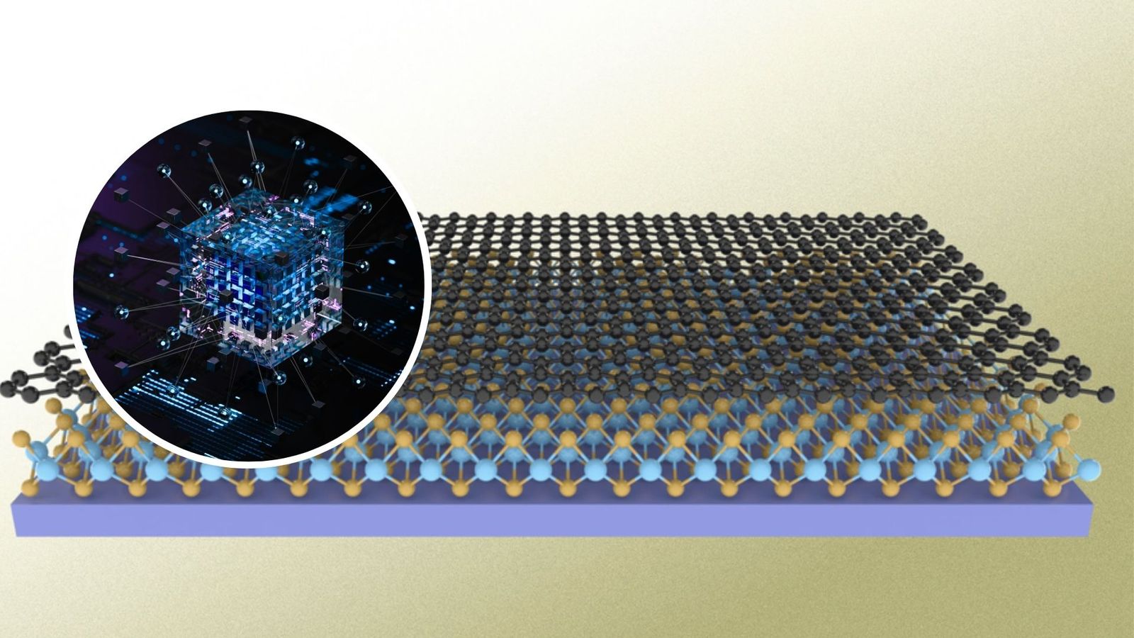
Researchers from the Massachusetts Institute of Technology (MIT) and collaborators have developed a method to produce large, uniform areas of ultrathin superconducting material. This material, niobium diselenide, is grown beneath a layer of graphene, an atomically thin carbon-based material. The graphene layer protects the superconductor from oxidation and facilitates its growth over a large wafer-scale area.
Xudong Sheldon Zheng, a graduate student in MIT's Department of Electrical Engineering and Computer Science, co-leads this study. He notes that the new process enables the production of monolayer superconductors at a scale previously unattainable. This advancement opens opportunities for studying these materials, integrating them into circuits, and exploring practical applications. The research team successfully integrated the air-stable superconductor into a superconducting microwave circuit, where it maintained its superconducting properties and exhibited high kinetic inductance, beneficial for quantum devices.
The development could lead to more compact superconducting quantum computing hardware and technologies like ultrasensitive quantum detectors. Niobium diselenide, composed of a single layer of niobium atoms between selenium atoms, offers high kinetic inductance, allowing it to store significant inductive energy in a small area. This characteristic is desirable for many quantum devices. The study, published in Nature, describes an 'encapsulation epitaxy' mechanism that facilitates the growth of large-area, air-stable monolayer niobium diselenide films and their potential in superconducting quantum circuits.
This research demonstrates a unique growth phenomenon where a 2D encapsulation layer, such as graphene, pre-deposited on a 3D substrate, serves as both a template for the epitaxial growth of niobium diselenide and a protective layer against degradation. Zheng explains that typically, once the material is exposed to air, it begins to oxidize and degrade. However, the new method overcomes this challenge, allowing for reliable device fabrication at the wafer scale, unlike previous methods that relied on exfoliation techniques yielding small flakes.
Source: Graphene Feed