News12 October 2026· Graphene Feed
Ultraviolet laser creates flexible circuits from waste materials
GrapheneElectronicsSensorsOptoelectronicsPackagingSustainabilityResearch & InnovationSupply Chain
74 articles on Graphene in Sensors.
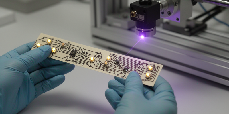
Researchers at the National University of Singapore have developed a method to create laser-induced graphene circuits on kraft paper using a 355-nanometer ultraviolet laser, enabling flexible, biodegradable electronics.
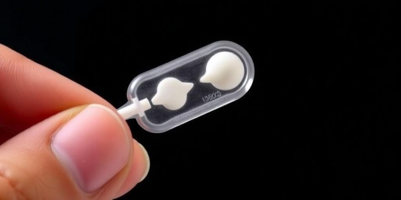
Researchers have developed Lollylab, a lollipop-shaped device that measures acetaminophen levels in saliva in under two minutes using a graphene sensor, offering a noninvasive testing method.
Researchers developed a cost-effective method to integrate graphene oxide into contact lenses, enhancing smart vision capabilities while remaining compatible with current manufacturing processes.

Researchers from Peking University, Tsinghua University, and the University of Hong Kong developed graphene reservoirs to precisely control ice thickness in cryo-electron microscopy, achieving uniform depths as thin as 15 nanometers.
Global Graphene Group seeks a Sales Engineer in Dayton, Ohio, to expand its graphene markets. Apply by December 31, 2026.
Researchers at Khalifa University reviewed how graphene enhances high-density polyethylene (HDPE). They examined compounding techniques and found that graphene improves HDPE's thermal, electrical, and barrier properties when well-dispersed.
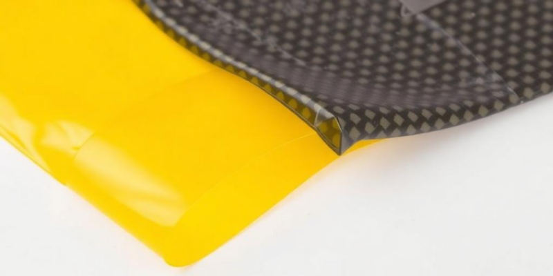
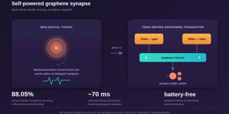
Researchers developed a flexible graphene neural interface that mimics synapses, integrating transistors and rGO electrodes for wearable sensing applications.
First Graphene and Vector have partnered to launch PureGRAPH® heat sensors.
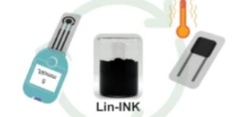
Researchers have demonstrated that few-layer graphene recovered from used sensors can be reprinted up to five times without losing performance.
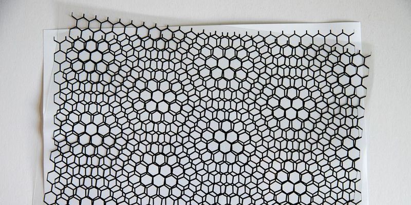
Researchers have published two studies cataloging nearly 9,000 two-dimensional materials, identifying over 1,600 candidates for twisting to create new quantum simulators.

Researchers have developed miniaturized biosensor platforms capable of detecting neurodegenerative disease biomarkers, such as amyloid-beta and tau proteins, at extremely low concentrations, potentially enabling earlier diagnosis.

Researchers have developed a method to synthesize nanographenes with up to eight helicenes, each with controlled handedness. This allows for precise tuning of optical and electronic properties.

The Advanced Carbons Council calls for a U.S. carbon materials innovation platform focused on standards, testing and buyer qualification. The paper links engineered-carbon supply chains to manufacturing, energy, defense and AI infrastructure. Serves as a model for governments world-wide.
Researchers are studying exotic quantum phases in 2D nanomaterials by twisting them into moiré superlattices, with superconductivity in graphene observed at a 1.1° twist angle.
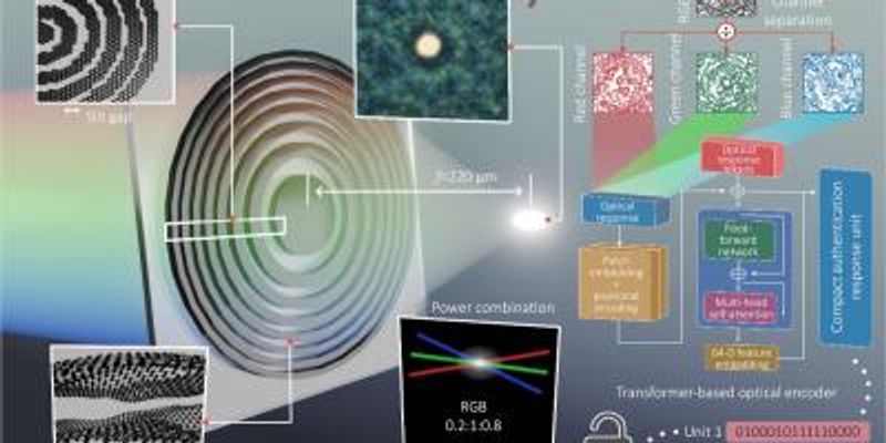
Yonsei University researchers created graphene diffractive zone plates that convert light patterns into unclonable binary security keys using a vision transformer-based model. The system shows promise for optical authentication.
Iowa State University researchers developed a method to print electronic circuits on 3D objects using aerosol-jet printing. NASA supports the commercialization with a $150,000 grant.
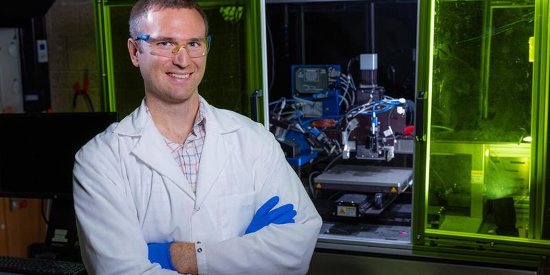
Researchers have designed a graphene oxide-based SPR sensor for detecting mercury, lead, and zinc in water. The simulated sensor achieved angular sensitivities up to 338°/RIU.
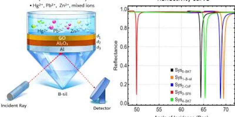
Researchers found that tiny wrinkles in graphene can alter its electrical properties. This discovery could lead to advanced control of electricity in ultrathin materials, enhancing sensor and electronic device performance.
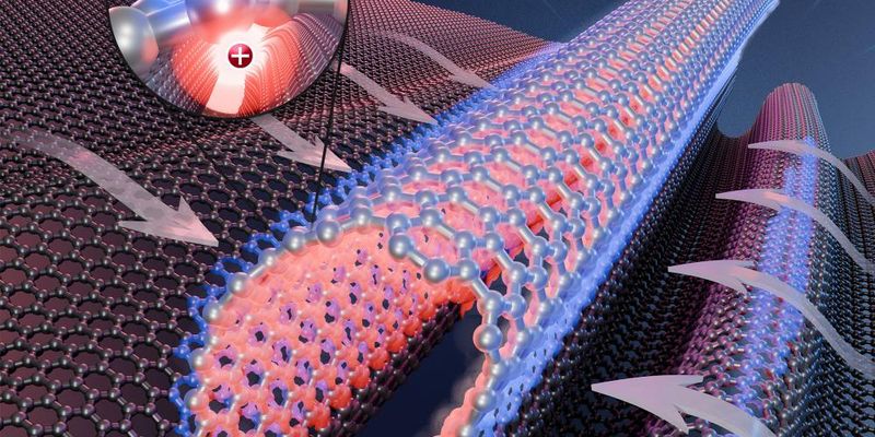
South Korean researchers developed a graphene nanomesh for wearable gas sensors, achieving six times higher sensitivity than flat graphene sensors. The design maintains flexibility and breathability for mask integration.
Researchers have developed graphene multielectrode arrays for versatile extracellular measurements, enhancing electronic biosensing capabilities.

The Graphene Engineering Innovation Centre offers roll-to-roll CVD systems for continuous graphene production, processing foils up to 15 cm wide at 5 metres per hour.
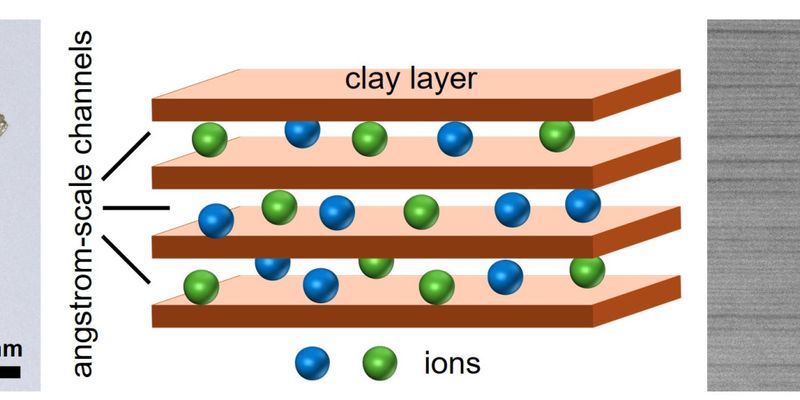
Researchers at the National Graphene Institute demonstrated that vermiculite clay channels can control ion flow in response to pressure, voltage, and pH, mimicking biological ion channels.
Romanian researchers developed a disposable graphene–copper sensor that detects lysine enantiomers in whole blood at concentrations as low as one attomole per litre, aiding cancer diagnostics.
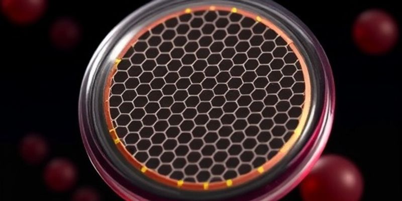
Paragraf has introduced a 12-channel graphene-based FET platform, featuring a real-time reader for enhanced performance in graphene electronics applications.
Researchers in the US and UK observed flexoelectricity in graphene, finding that extremely sharp bends create significant electrical polarization. This discovery aligns with theoretical predictions from 2008.
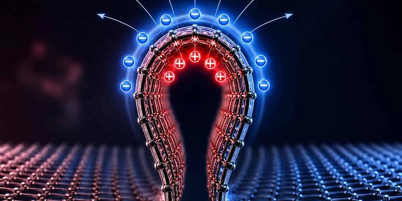
Researchers at Rice University demonstrated that graphene nanowrinkles can alter electrical properties, potentially enabling new applications in chemical and biological sensing.

A team from Duisburg-Essen and Uppsala universities has directly observed rainbow scattering in graphene using xenon ions, confirming a previously unmeasured phenomenon.
Researchers at EPFL developed a graphene device to measure fractional electric charges in quasiparticles during the quantum Hall effect, revealing charges of one-third and two-thirds of an electron.
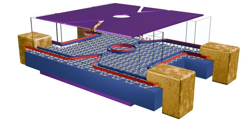
Researchers at Shanghai University and Shanghai General Hospital have built an electrochemical biosensor pairing a three-dimensional graphene framework with a heat-denatured casein interlayer to detect uric acid in sweat at femtomolar levels.
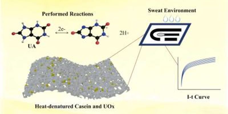
Paragraf has introduced a new graphene-based sensing platform and data acquisition system designed for enhanced sensor performance.
A team at the National University of Singapore has turned magic-angle twisted bilayer graphene from an insulator into a metal using only faint long-wavelength light, pointing to a new class of terahertz and far-infrared detectors.
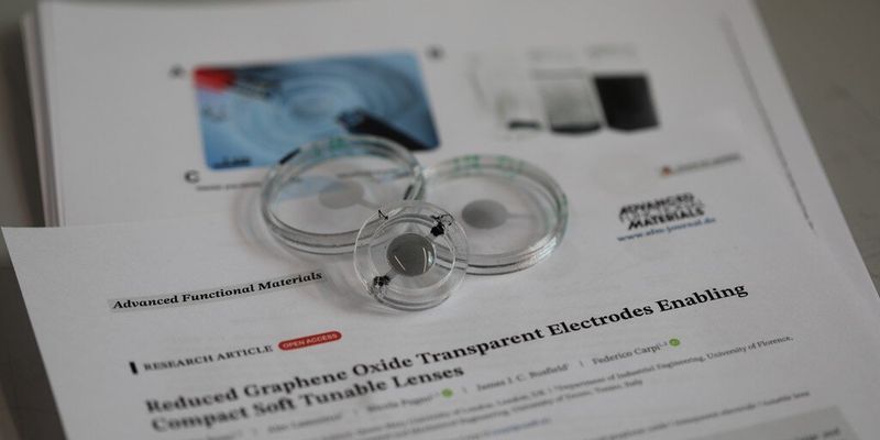
Researchers at Queen Mary University of London have developed a graphene-based soft lens that can electronically change focus without bulky parts, potentially advancing medical devices and cameras.
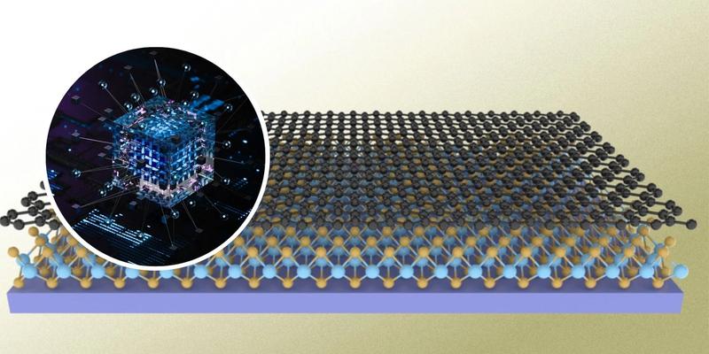
MIT researchers have developed a method to grow large, air-stable niobium diselenide films using graphene encapsulation. This advance could lead to more compact superconducting quantum devices.
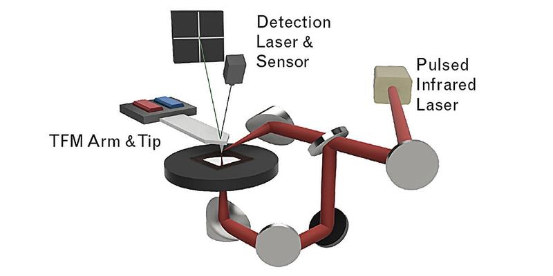
Researchers at the University of Maryland developed infrared torsional force microscopy, enabling near-nanometer precision imaging of material surfaces responding to infrared light.
Researchers, including MSE assistant professor Zafer Mutlu, are using graphene nanoribbons to create sensors capable of tracking extreme radiation levels.
Researchers incorporated thermally exfoliated graphene oxide into PVDF, enhancing both piezoelectric and triboelectric responses. This nanocomposite could advance self-powered wearables and flexible sensors.
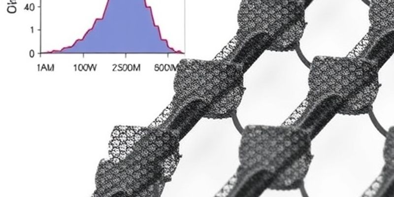
Researchers explain how optothermal Raman thermometry measures thermal conductivity in graphene by using laser-induced temperature changes. The method's accuracy depends on precise absorbed-power measurements.
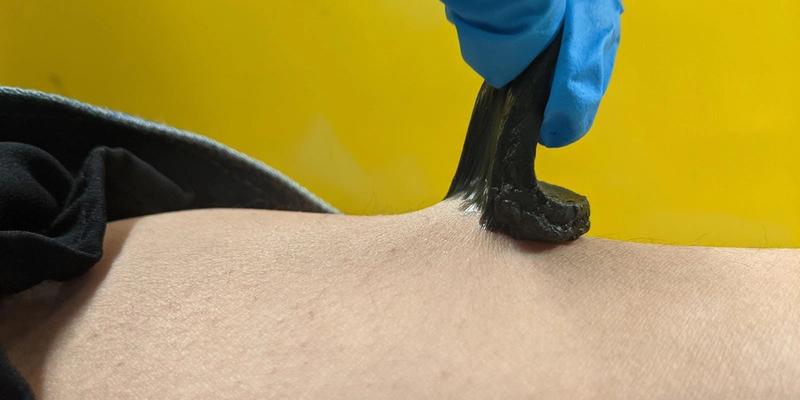
Drexel and Penn State researchers created a new hydrogel for biosensors that maintains skin contact through sweat and hair, enhancing durability and comfort during physical activity.
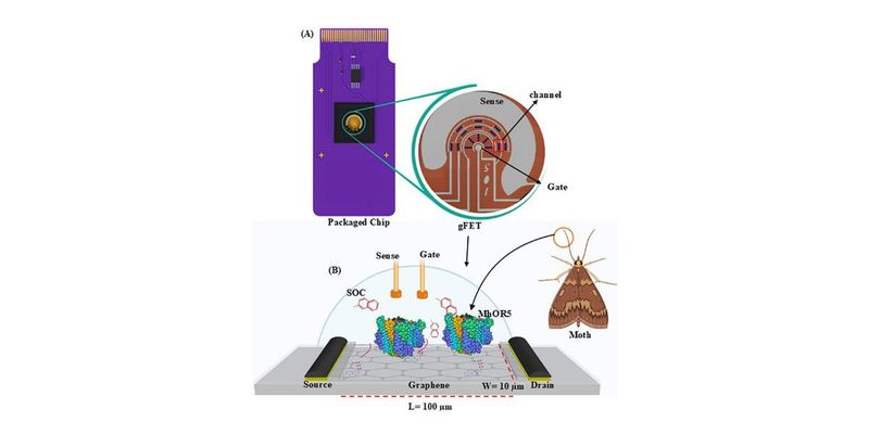
Bioengineers at UC San Diego integrated an insect olfactory receptor into graphene chips, creating a sensor that detects diverse organic compounds. This could lead to scalable, nature-inspired chemical sensors.
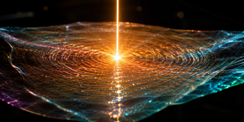
Researchers at ICREA have integrated semiconducting nanoporous graphene into sensing devices, using on-surface synthesis to build architectures that carry a usable bandgap.
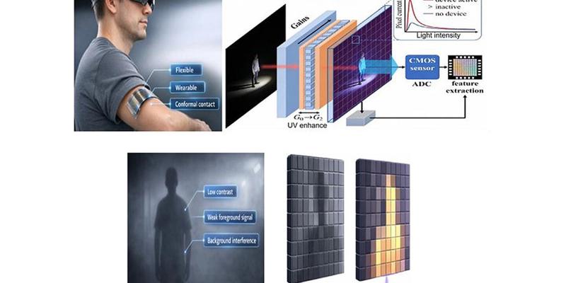
Researchers created a flexible memristor using perovskite quantum dots and graphene oxide, improving low-light image recognition by over 10% and doubling the signal-to-noise ratio.
Researchers at the University of Arizona demonstrated that graphene nanoribbons can withstand gamma radiation, suggesting their potential use as radiation sensors in fusion reactors and deep space applications.
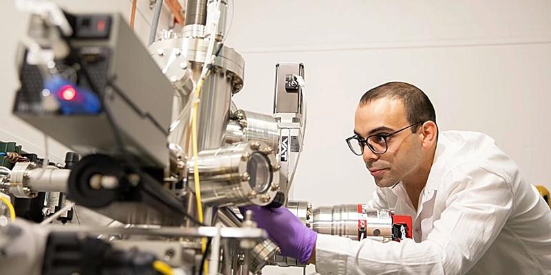
Researchers at two London universities used QuEra's Aquila device to validate a method for extracting thermodynamic properties from nitrogen-doped graphene, tested on a 78-site system.
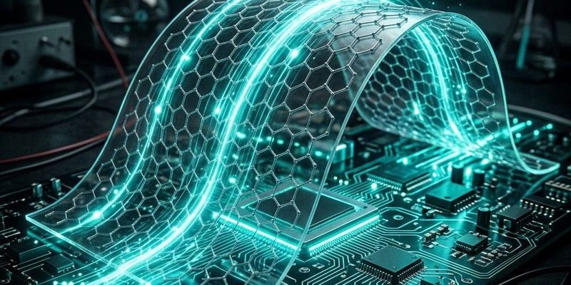
In a video, HydroGraph CEO Kjirstin Breure discusses how their graphene enabled a biosensor company to create technology that wasn't possible with other commercially available graphenes.

Researchers at Nagoya University have developed a technique to dynamically reshape graphene oxide nanofilms using computer-controlled electricity. This advancement could enhance the versatility of graphene-based materials in applications requiring precise 3D structures.

Researchers at Penn State have developed a battery-free solar computing chip that integrates silicon photovoltaics, MoS₂/WSe₂ complementary logic, and graphene chemical sensors. This innovation highlights the potential of graphene in enhancing the efficiency and functionality of solar-powered computing devices.
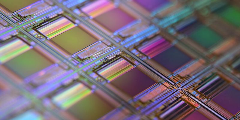
Researchers at Helmholtz-Zentrum Berlin have developed a new perovskite solar cell by incorporating graphene, enhancing its durability and efficiency. This advancement in perovskite technology could significantly reduce production costs and improve the performance of solar cells, potentially increasing the adoption of lightweight, flexible solar solutions over traditional silicon-based panels.

Researchers from Brazil's Federal University of Pelotas and Federal University of Rio Grande do Sul have developed a laser-induced graphene sensor capable of detecting dopamine in tear fluid with high sensitivity. This advancement could lead to noninvasive monitoring of neurological disorders, utilizing the electroactive properties of graphene to provide a compact and scalable alternative to traditional methods that often require blood or implanted devices.
Researchers at the Helmholtz-Zentrum Berlin, along with collaborators, have developed a perovskite solar cell with a graphene-oxide interface that achieves 27.3% power conversion efficiency and maintains over 90% of this efficiency after 770 hours of operation. This advancement addresses the stability issues in all-perovskite triple-junction cells, potentially paving the way for more durable and efficient solar technologies using carbon-based materials like graphene.
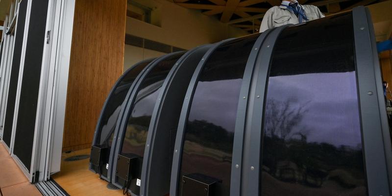
Researchers used a laser to convert portions of a thin plastic film into electrically conductive graphene to create a sensor. This development could lead to new applications for graphene in biomedical devices, particularly in analyzing biological fluids like tears.
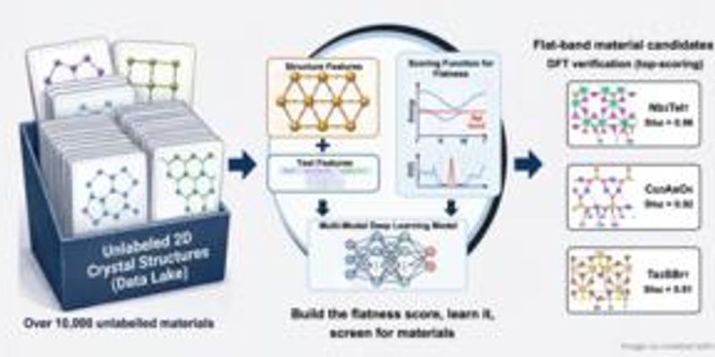
Dr Qian Yang at the National Graphene Institute, University of Manchester, has developed a new learning tool to expedite the search for two-dimensional quantum materials. This advancement could accelerate the discovery and application of graphene and other 2D materials in various technologies.
Researchers have developed a graphene-based sensing platform designed for rapid detection of PFAS. This advancement could enhance monitoring efforts by utilizing graphene's sensitivity and conductivity properties to provide quicker analysis at the point of need.

Turquoise Group has achieved Verified Graphene Producer® status, confirming its capability to produce 30 tonnes of high-purity few-layer graphene annually at its Brisbane facility. This certification enhances the company's credibility in delivering high-quality graphene, a material crucial for applications in coatings, composites, and energy storage.

Researchers at MIT have discovered that rhombohedral graphene can host multiple superconducting states simultaneously, with some states becoming stronger under magnetic fields. This finding is significant for advanced carbon materials as it reveals new possibilities for manipulating graphene's superconducting properties, which could impact quantum computing and other technologies relying on superconductivity.
Researchers at Concordia University have developed nanocomposites using graphene oxide and reduced graphene oxide embedded in a nanocellulose matrix, achieving high accuracy in predictive modeling with R² > 0.99. This advancement is significant for the field of advanced carbon materials as it demonstrates the potential of these composites in applications such as wearable electronics and biosensors, leveraging the unique properties of graphene oxide and reduced graphene oxide.
European semiconductor companies raised substantial funding in 2025, with the ten largest rounds ranging from NXP Semiconductors' €1 billion EIB loan down to IQE's £18 million convertible note, spanning AI chips, photonics, power electronics, memory, and chip cooling. Two graphene-focused companies, Paragraf ($55M Series C) and CamGraPhIC (€25M Series A), secured funding to scale graphene-based electronic devices and graphene silicon photonics respectively, signaling continued investor commitment to graphene's commercial role in semiconductors and optical interconnects.

Researchers applied the Small Perturbation Method to analytically and numerically model how Gaussian surface roughness affects bistatic scattering coefficients, transmission coefficients, and shielding effectiveness for copper and graphene slabs across radio-frequency to near-infrared ranges. The findings provide design guidelines for tuning graphene-based shielding and optical devices by adjusting chemical potential, temperature, and layer count alongside surface roughness parameters.
Researchers at ICN2, led by Jose A. Garrido, are developing graphene-based thin film devices for neural stimulation and recording, with work spanning device fabrication, in vivo testing in rodent and large-animal models, and clinical translation efforts. The work demonstrates a pathway for graphene to move from laboratory research into regulated medical devices, advancing the material's role in bioelectronics beyond conventional carbon fiber or composite applications.
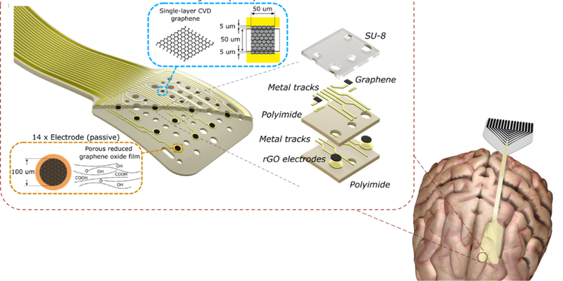
INBRAIN Neuroelectronics completed enrollment of ten patients (eight treated) in a first-in-human trial of its graphene cortical interface, conducted during brain tumor resection surgeries at Northern Care Alliance NHS Foundation Trust, with no device-related adverse events or perioperative failures observed. The results support graphene as a viable electrode material for neural interfaces, with implications for the graphene sector as the technology advances toward clinical commercialization in brain-computer interface applications.
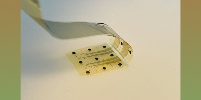
Professor Roman Gorbachev at the University of Manchester received a £1.9 million EPSRC Open Fellowship to lead a five-year project scaling van der Waals 2D material heterostructures from micrometre samples to wafer-scale fabrication using a new ultra-high vacuum platform. The work directly advances graphene and 2D materials manufacturing by targeting industrial-process compatibility and establishing a UK fabrication hub accessible to academic and industry users.

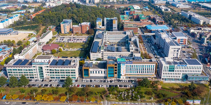
Gyeongsangbuk-do Province secured 30 billion won in South Korean state funds across three projects targeting graphene 2D nanomaterials, ultra-precise electronic glass, and on-device AI for manufacturing, running from 2026 to 2030. The graphene project, organized by POSTECH Nano Convergence Technology Institute with 14.3 billion won, aims to build Korea's first end-to-end infrastructure covering graphene synthesis through to commercialization, addressing the country's longstanding gap between R&D capability and industrial-scale production.
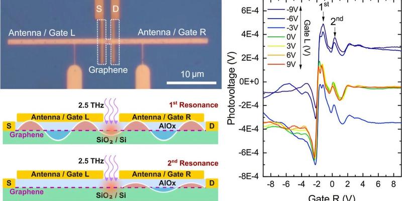
Researchers at ICFO and partner institutions built a monolayer graphene terahertz photodetector using acoustic graphene plasmon cavities grown via chemical vapor deposition, achieving a 30% higher photoresponse than conventional devices without hexagonal boron nitride encapsulation, published in ACS Photonics in 2026. The result shows that CVD-grown graphene can deliver competitive THz detection performance without the fabrication complexity of hBN encapsulation, lowering a barrier to large-scale graphene device manufacturing.
Canada's graphene sector has developed across production, construction, filtration, printed electronics, and energy storage, with companies such as NanoXplore operating a 4,000-metric-ton-per-year facility in Montréal and firms like Zentek and Graphene Leaders Canada advancing application-specific products toward commercial deployment. The ecosystem signals a shift from materials science demonstration toward repeatable industrial use cases in carbon-based composites, conductive additives, and separation technologies, though commercial viability still depends on product qualification, standardization, and cost competitiveness against incumbent materials.

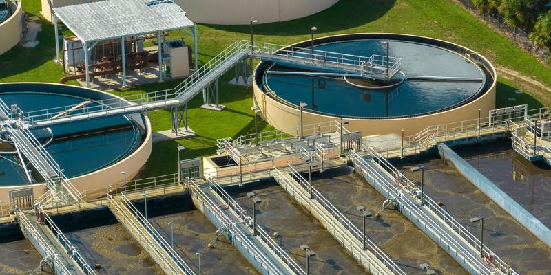
Researchers and engineers are evaluating graphene oxide and reduced graphene oxide as adsorbents, antifouling coatings, catalytic supports, and modified membrane layers within industrial water treatment systems targeting COD removal, biofouling control, and reverse osmosis feed protection. The graphene sector faces a clear scaling challenge, as industrial adoption of these carbon nanomaterials depends on demonstrating mechanical stability, resistance to chemical cleaning cycles, controlled delamination, and validated cost-per-cubic-meter performance in pilot tests using real effluent matrices.
Terrance Barkan of the Advanced Carbons Council and Dr. Andrew Pollard of the UK's National Physical Laboratory discussed how measurement science, standardization, and materials verification underpin the commercialization of graphene and other advanced carbon materials. For the sector, the conversation highlights that without validated characterization methods and traceable measurement standards, reproducible manufacturing and scalable deployment of carbon nanomaterials — including graphene, carbon nanotubes, and emerging MXenes — remain unachievable.
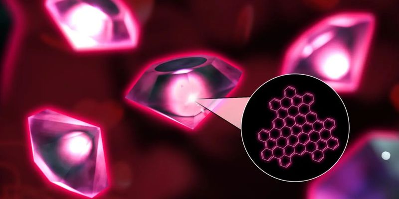
A team led by Yingke Wu and Tanja Weil at the Max Planck Institute for Polymer Research synthesized 3–4 nm nanodiamonds from nanographene building blocks under high pressure and temperature, publishing the results in Nature. The bottom-up method gives precise control over nanodiamond size and allows silicon- and germanium-based optical emitters to be incorporated during synthesis without post-processing, which is relevant for carbon-based quantum and photonic material development.
Researchers at Vietnamese universities fabricated a glassy carbon electrode modified with poly(pyrocatechol violet) and electrochemically reduced graphene oxide using one-step cyclic voltammetry, achieving a metronidazole detection limit of 0.013 µM. The work demonstrates a route to functionalized reduced graphene oxide composites that avoids toxic chemical reductants, relevant to the development of graphene-based electrochemical sensing materials.

Researchers at the Max Planck Institute for Polymer Research, led by Yingke Wu and Tanja Weil, synthesized nanodiamonds of 3–4 nanometers from graphene fragments using high pressure and high temperature, publishing the results in Nature. The bottom-up method allows precise control over nanodiamond size, structure, and dopant atoms—such as nitrogen for vacancy centers or silicon for photoluminescence—which is relevant for graphene-derived carbon nanomaterials and quantum photonics applications.
Researchers at Brookhaven National Laboratory used a 36 Tesla magnet to observe a previously unknown flat-band state in pristine graphene that emerges at integer multiples of an applied magnetic field, publishing the findings in Physical Review Letters. The tunable band structure could inform the design of graphene-based Hall sensors and resistance metrology standards.

Researchers from the University of Warwick, University of Nottingham, and Diamond Light Source grew graphene films with controllable defect densities using a molecule called azupyrene, which naturally incorporates five- and seven-membered carbon rings, with defect levels tuned by growth temperature. The method gives the graphene sector a reproducible route to engineer surface reactivity, with direct implications for graphene-based catalysts and gas sensors.
A research team at Osaka University built a graphene nanoribbon-based gas sensor capable of detecting individual CO2 molecules at ambient pressure, achieving detection limits below 10 parts per trillion, as published in Nature Materials. The result demonstrates graphene nanoribbons as a viable platform for ultra-sensitive gas detection, with potential applications in environmental monitoring and medical breath analysis.

A team at the National University of Singapore developed a graphene field-effect transistor biosensor that detects four oral cancer biomarkers from saliva in 90 seconds, achieving 94.2% sensitivity and 91.8% specificity in a 220-patient clinical pilot. The device demonstrates a scalable diagnostic application for functionalized graphene, with a spinout company pursuing commercialization and a projected per-test cost under 4 USD.
The University of Exeter's Centre for Graphene Science demonstrated a graphene-zinc oxide heterostructure UV photodetector with an 8-nanosecond response time at 365 nm, 10x faster than commercial silicon devices, as published in Advanced Materials. The result advances graphene's case as a functional material in high-speed optoelectronics, with Hamamatsu Photonics engaged for industrial-scale validation and patents filed across three jurisdictions.

Premier Graphene Inc and Mitsubishi Pencil Company signed a joint development agreement to co-develop graphene-based conductive inks for printed electronics, targeting two co-branded product launches in late 2026 with a combined first-year revenue target of 12 million USD. The deal advances commercial adoption of single-layer graphene dispersions in printed electronics applications such as RFID tags, smart packaging, and biosensor electrodes.